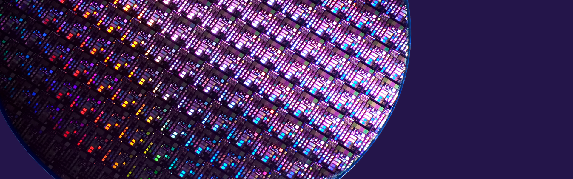
碳化硅与第三代半导体
元介技术的 unique water jet guided laser systems offer many advantages for applications in the semiconductor industry compared to conventional diamond blade saws or laser systems. The Laser MicroJet® combines the accuracy of a laser with the cooling and guiding capabilities of a thin water jet. This unique approach results in smooth edges, high wafer fracture strength, and less risk of breakage.
The LMJ is ideally suited for processing a wide range of semiconductor materials, including silicon (Si), silicon carbide (SiC), low-K materials and even coated materials such as Epoxy molded compound wafers of various thicknesses. Thanks to its minimal thermal impact, the LMJ ensures that material integrity is preserved throughout the entire cutting process.
Typical semiconductor applications include wafer downsizing, wafer trimming, edge grinding, and wafer dicing. The LMJ is also used for processing semiconductor equipment and consumables, including hole drilling, slot cutting, etching, and the machining of special shapes.
可加工材料
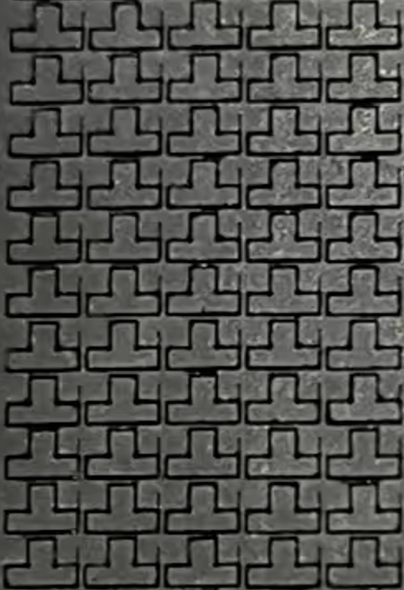
红外水导激光可加工碳化硅、氮化镓、氧化铝、蓝宝石等硬脆材料,切缝窄、无崩边。y.
碳化硅(SiC)
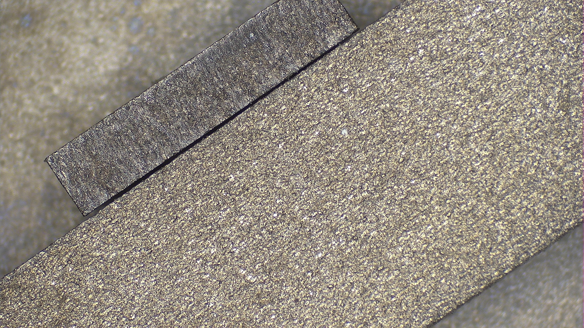
第三代半导体材料:SiC、GaN、AlN;可实现切缝窄(≤20μm)、边缘无崩边的精密切割。
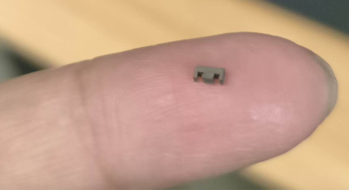
应用场景
SiC、GaN晶圆的超薄切割与划片,提升芯片良率,满足高频高压器件需求。
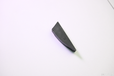
典型应用
SiC晶圆切割
超薄切割与划片
GaN晶圆加工
高频高压器件制造
陶瓷基复合材料加工
Silicon
蓝宝石切割
CMC精密加工
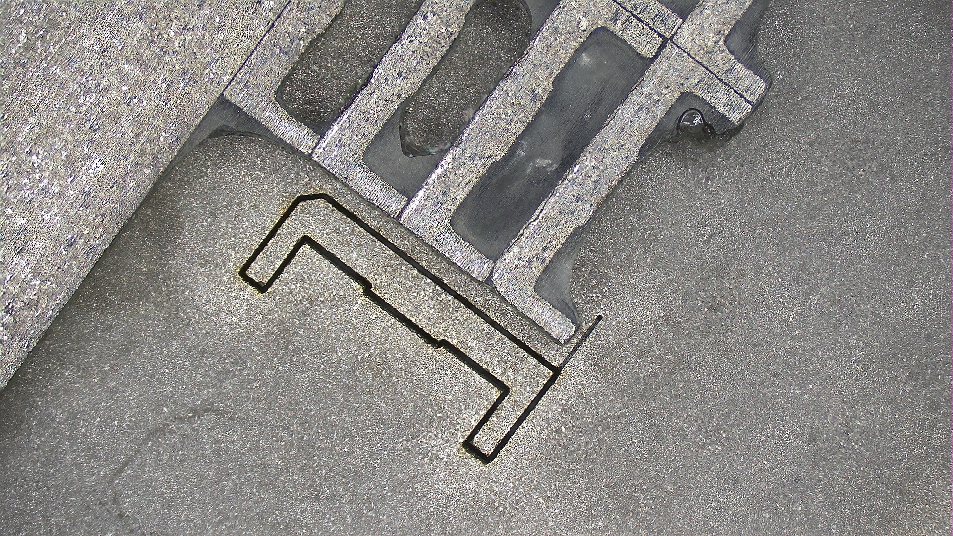
气膜冷却孔钻削
Silicon carbide
预约打样演示
填写表单,我们将尽快与您联系。